The connector additionally contains signals that are specific to Poqet. Any signals marked as reserved must be left unconnected, since they are for manufacturing use only, or are intended for future enhancements of the bus.
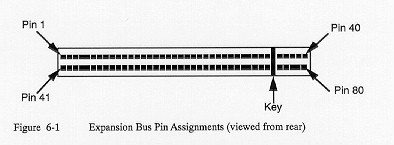
Table 6-1 lists the PQXT Expansion Bus signals by pin and function.
Table 6-1: Expansion Bus Pins Assignments
PIN  SIGNAL     DIR    DESCRIPTION
---  ---------  -----  --------------------------------------------------------
  1  GND        -      System Logic Ground.  This line must be used by external
                       devices to guarantee a common ground reference.
  2  SRESET     O      System Reset.  Used to reset or initialize the system
                       logic when the Reset Button on the keyboard is
                       depressed.
  3  VDD(1)     O      Power supply output voltage.  Supplies the positive
                       voltage from the PQXT power supply.  There are extreme
                       limits on the use of this pin.  The power drain lim-
                       itations are explained later in this chapter.
  4  IRQ2       I      Interrupt Request 2.  Used to signal the microprocessor
                       that an I/O device needs attention.  The request is
                       generated by bringing the IRQ2 line to a high level from
                       a low level and holding it high until it is acknowledged
                       by the microprocessor.
  5  Reserved   -      Do not use.  This pin would normally be used for -5V on
                       a standard XT system.  -5V is not supported in the PQXT.
  6  DRQ2       I      DMA Request 1.  This line is used by a peripheral device
                       to gain access to the DMA service of PQXT.  It is gen-
                       erated by bringing the DRQ2 line to a high level and
                       leaving it there until the DACK2 line goes active.
  7  Reserved   -      Do not use.  This pin would normally be used for -12V on
                       a standard XT system.  -12V is not supported in the
                       PQXT.
  8  Reserved   -      Do not use.
  9  Reserved   -      Do not use.  This pin would normally be used for +12V
                       on a standard XT system.  +12V is not supported in the
                       PQXT.
 10  GND(1)     -      See description for pin 1 (GND) above.
 11  MEEMWN     O      Memory Write Command.  Instructs the memory device to
                       store the data that is present on the data bus.
                       Active low.
 12  MEMRN      O      Memory Read Command.  Instructs the memory device to
                       place its data on the data bus.  Active low.
 13  IOWN       O      I/O Write Command.  Instructs the I/O device to store
                       the data present on the data bus.  Active low.
 14  IORN       O      I/O Read Command.  Instructs the I/O device to place its
                       data on the data bus.  Active low.
 15  DACK3N     O      DMA Acknowledge 3.  Used to acknowledge the DRQ3.
                       Active low.
 16  DRQ3       I      See description for pin 6 (DRQ2) above.
 17  DACKLN     O      See description for pin 15 (DACK3N) above.
 18  DRQ1       I      See description for pin 6 (DRQ2) above.
 19  Reserved   -      Do not use.  This pin would normally be used for DRAM
                       refresh on a standard XT system.  DRAM refresh is not
                       supported in the PQXT.
 20  SYSCLK     O      System Clock.
 21  IRQ7       I      Similar to IRQ2 above.
 22  IRQ6       I      Similar to IRQ2 above.
 23  IRQ5       I      Similar to IRQ2 above.
 24  Reserved   -      Do not use.  This pin would normally be used for IRQ4
                       on a standard XT system. IRQ4 is not supported in the
                       PQXT. This pin is used internally for the PQXT com-
                       munications port and must be left open.
 25  IRQ3       I      Similar to IRQ2 above.
 26  DACK2N     O      Similar to DACK3N above.
 27  TC         O      Terminal Count.  Generates a pulse when the DMA channel
                       being used has reached its terminal count. Active high
 28  SALE       O      Address latch Enable.  Provided on the I/O channel as
                       an indicator of a valid address-when used with the AEN
                       signal. The address is latched on the falling edge of
                       ALE.
 29  VDD(1)     O      See VDD description above (pin 3).
 30  Reserved   -      Do not use.  This pin would normally be used for a
                       14.31818 MHz clock signal on a standard XT system. This
                       clock line is not available in the PQXT. Any peripheral
                       that requires it must generate it in the	expansion card.
 31  GND(1)     -      See description for pin 1 (GND) above.
 32  TxD(2)     O      Transmit Data
 33  RTS(2)     O      Request to Send
 34  DTR(2)     O      Data Terminal Ready
 35  KEY        -      Used to ensure proper mating connector orientation.
 36  RxD(2)     I      Receive Data.
 37  CTS(2)     I      Clear to Send
 38  DSR(2)     I      Data Set Ready
 39  DCD(2)     I      Data Carrier Detect
 40  BATT(1)    I      Battery Voltage.  Used to externally power the PQXT
                       during manufacturing test and burn-in.  This pin is
                       connected directly to the battery terminals and must
                       never be connected to expansion devices.
Warning! Connecting an external power source to this pin with
the batteries installed can cause the batteries to EXPLODE, causing
internal system damage and/or personal injury.
 41  IOCHCKN(1) I      I/O Channel Check.  Provides the microprocessor with
                       error information on the I/O channel.  When this pin
                       is low, an error is indicated.
 42  EXPP7(D7)  I/O    Data Bit 7.  This line provides bit 7 of the data bus
                       for the I/O expansion channel.  Bidirectional.
 43  EXPP6(D6)  I/O    See description for pin 42 (EXPP7) above.
 44  EXPP5(D5)  I/O    See description for pin 42 (EXPP7) above.
 45  EXPP4(D4)  I/O    See description for pin 42 (EXPP7) above.
 46  EXPP3(D3)  I/O    See description for pin 42 (EXPP7) above.
 47  EXPP2(D2)  I/O    See description for pin 42 (EXPP7) above.
 48  EXPP1(Dl)  I/O    See description for pin 42 (EXPP7) above.
 49  EXPP0(D0)  I/O    See description for pin 42 (EXPP7) above.
 50  IOCHRDY    I      I/O Channel Ready.  When this open drain pin is pulled
                       low (not ready) by an I/O channel device, the memory or
                       I/O cycle that is currently taking place will become
                       lengthened. Any slow external device should drive this
                       line low immediately upon detecting a valid address and
                       a read or write command. Machine cycles are extended an
                       intergal number of SYSCLK cycles when this line is
                       active as described above.
 51  AEN        O      Address Enable. Used to de-gate the processor and other
                       devices from the I/O channel during a DMA cycle.
                       Active high.
 52  SA19       O      System Address Bit 19.  Used to address the memory and
                       I/O devices within the system. One MB of memory can be
                       accessed with address bits SA0-19.
 53  SA18       O      See description for pin 52 (SA19) above.
 54  SA17       O      See description for pin 52 (SA19) above.
 55  SA16       O      See description for pin 52 (SA19) above.
 56  SA15       O      See description for pin 52 (SA19) above.
 57  SA14       O      See description for pin 52 (SA19) above.
 58  SA13       O      See description for pin 52 (SA19) above.
 59  SA12       O      See description for pin 52 (SA19) above.
 60  SA11       O      See description for pin 52 (SA19) above.
 61  SA10       O      See description for pin 52 (SA19) above.
 62  SA9        O      See description for pin 52 (SA19) above.
 63  SA8        O      See description for pin 52 (SA19) above.
 64  SA7        O      See description for pin 52 (SA19) above.
 65  SA6        O      See description for pin 52 (SA19) above.
 66  SA5        O      See description for pin 52 (SA19) above.
 67  SA4        O      See description for pin 52 (SA19) above.
 68  SA3        O      See description for pin 52 (SA19) above.
 69  SA2        O      See description for pin 52 (SA19) above.
 70  SA1        O      See description for pin 52 (SA19) above.
 71  SA0        O      See description for pin 52 (SA19) above.
 72  Reserved   -      Do not use. This pin supports Poqet-specific functions.
                       It is of no use to any I/O channel device and must be
                       left unconnected.
 73  Reserved   -      Do not use. This pin supports Poqet-specific functions.
                       It is of no use to any I/O channel device and must be
                       left unconnected.
 74  Reserved   -      Do not use. This pin supports Poqet-specific functions.
                       It is of no use to any I/O channel device and must be
                       left unconnected.
 75  KEY        -      Used to ensure proper mating connector orientation.
 76  Reserved   -      Do not use. This pin supports Poqet-specific functions.
                       It is of no use to any I/O channel device and must be
                       left unconnected.
 77  Reserved   -      Do not use. This pin supports Poqet-specific functions.
                       It is of no use to any I/O channel device and must be
                       left unconnected.
 78  EMCS3(1)	O      ROM Chip Select.  For manufacturing test use only.
                       No connection may be made to this line by an I/O
                       expansion device.
 79  MRESETN(1) I      Master Reset.  Pulling this pin low is equivalent to
                       pressing the Master Reset pin on the system keyboard.
                       The entire system will reset itself and all data will
                       be lost.  It it normally used only during manufacturing
                       test, but you may use it to reset the system.  However,
                       extreme care should be exercised before activating this
                       signal.  A minimum pulse width of 5 microseconds is
                       recommended.
 80  DISEXPP(1) O      Disable Expansion Bus.  When this line is high, no
                       device on the expansion bus is allowed to drive the
                       data bus (EXPP0-7).  This pin must be incorporated into
                       any external memory decoding logic to ensure that no
                       memory device is accessed while the line is high.

     Note:      In Table 6-1, all signals are standard XT signals except as
                noted:

                1 = Poqet-specific signal
                2 = RS-232-C signal
Table 6-2: RS-232C Pin Assignments
   PIN  SIGNAL  I/O  DESCRIPTION
   ---  ------  ---  ---------------------
    32  TxD      O   Transmit Data
    33  RTS      O   Request to Send
    34  DTR      O   Data Terminal Ready
    36  RxD      I   Received Data
    37  CTS      I   Clear to Send
    38  DSR      I   Data Set Ready
    39  DCD      I   Data Carrier Detect
Table 6-3: Reserved Pin Assigmnents
    PIN  SIGNAL    NORMAL USE
  -----  --------  ---------------------------------------
      5  Reserved  -5V on a standard XT system
      7  Reserved  -12V on a standard XT system
      8  Reserved  not used
      9  Reserved  +12V on a standard XT system
     19  Reserved  DRAM refresh on a standard XT system
     24  Reserved  IRQ4 on a standard XT system
     30  Reserved  14.3 Mhz clock on a standard XT system
  72-74  Reserved  not used-must be left unconnected
  76,77  Reserved  not used-must be left unconnected
Table 6-4: Poqet-Specific Pin Assigmnents
      PIN  SIGNAL   I/O  DESCRIPTION
  -------  -------  ---  ----------------------
       80  DISEXPP   O   Disable Expansion Bus
       79  MRESETN   I   Master Reset
       78  EMCS3     O   ROM Chip Select
       40  BATT      I   Battery Voltage
     3,29  VDD       O   Power Supply Output
  1,10,31  GND       -   System Logic Ground
Warning! If the voltages between the peripheral device and PQXT are mismatched, the PQXT batteries may experience excessive current drain, which may cause permanent system component damage.
If you plan on disabling the PQXT power management feature, set the peripheral supply voltage to 4.75V +/-5%. This matches the PQXT supply voltage.
Power management is enabled automatically each time the PQXT is turned on, and is shown by a black indicator bar above the * symbol at the bottom of the LCD display screen. Power management can be disabled by depressing the Poqet and F4 keys simultaneously so that the bar above the * symbol becomes empty. See Chapter 5, "Power Management," for more details on enabling and disabling power management.
Warning! Any input voltage greater than 7V will physically damage the PQXT.
Note: Even when the PQXT is powered externally, the PQXT AA batteries continue to supply power to the LCD display.
There is no reason why you cannot use this signal to reset the PQXT from an external source. Of course, you must exercise caution, as the PQXT will be initialized and all data in system memory and in the temporary storage on drive D will be lost when you activate this signal. MRESETN must be a CMOS open-drain signal only. The 8OC88 requires a minimum MRESETN reset pulse width of 4 clock pulses (approximately 600 ns). It is recommended that you provide an active low pulse of at least 5 microseconds. A better guideline is to make sure that the pulse is at least three times the minimum width to ensure proper operation over all environmental conditions.